| CPC H01L 29/732 (2013.01) | 20 Claims |
|
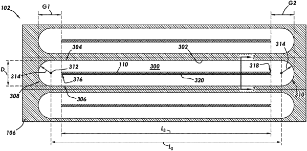
1. A semiconductor device comprising:
an emitter region defining an inner boundary in the shape of an obround with parallel sides, and the obround having a first hemispherical end and a second hemispherical end each having a radius;
a base region having a first end, a second end opposite the first end, and base length, the base region disposed within the obround with the base length parallel to and centered between the parallel sides, the first end spaced apart from the first hemispherical end by a first gap greater than the radius by more than a manufacturing tolerance, and the second end spaced apart from the second hemispherical end by a second gap greater than the radius by more than the manufacturing tolerance.
|