| CPC H01L 29/063 (2013.01) [H01L 21/0465 (2013.01); H01L 29/1095 (2013.01); H01L 29/1608 (2013.01); H01L 29/66068 (2013.01); H01L 29/7802 (2013.01)] | 15 Claims |
|
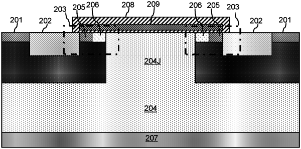
1. A silicon carbide MOSFET comprising:
a substrate heavily doped with a first conductivity type;
an epitaxial layer lightly doped with the first conductivity type having a junction field effect transistor (JFET) region of the first conductivity type;
a body region doped with a second conductivity type formed in the epitaxial layer wherein the second conductivity type is opposite the first conductivity type;
an accumulation mode region doped with the first conductivity type formed in the body region and an inversion mode region of the second conductivity type formed in the body region, wherein the accumulation mode region is located between the JFET region and the inversion mode region; and
a source region with the first conductivity type doped from a surface of the epitaxial layer to a depth deeper than a bottom of the inversion mode region.
|