| CPC H01L 27/0886 (2013.01) [H01L 21/02181 (2013.01); H01L 21/31144 (2013.01); H01L 21/32133 (2013.01); H01L 21/76802 (2013.01); H01L 21/76877 (2013.01); H01L 21/823431 (2013.01); H01L 21/823437 (2013.01); H01L 21/823468 (2013.01); H01L 21/823475 (2013.01); H01L 21/823821 (2013.01); H01L 23/5286 (2013.01); H01L 23/5329 (2013.01); H01L 23/62 (2013.01); H01L 27/0924 (2013.01); H01L 29/66545 (2013.01); H01L 29/66795 (2013.01); H01L 29/785 (2013.01)] | 22 Claims |

|
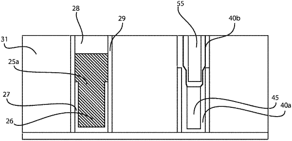
1. A method of forming a semiconductor structure, the method comprising:
forming a gate structure on first and second active regions of the semiconductor structure;
removing a portion of the gate structure to define a first gate structure on the first active region and a second gate structure on the second active region, wherein the first and second gate structures are in-line with one another and spaced apart by a gate cut trench;
forming a first etch stop layer in the gate cut trench;
forming a first dielectric material on the first etch stop layer in a lower portion of the gate cut trench;
forming a second etch stop layer on an upper surface of the first dielectric material; and
forming a second dielectric material on the second etch stop layer in an upper portion of the gate cut trench.
|