| CPC H01L 24/89 (2013.01) [H01L 21/50 (2013.01); H01L 21/67017 (2013.01); H01L 21/67103 (2013.01); H01L 24/75 (2013.01); H01L 2224/81065 (2013.01)] | 7 Claims |
|
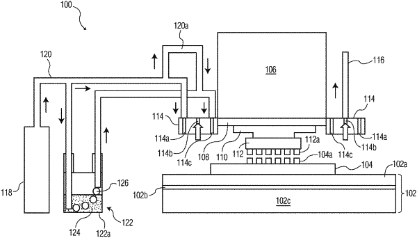
1. A bonding machine for bonding a semiconductor element to a substrate, the bonding machine comprising:
a bond head including a bonding tool, the bonding tool being configured to carry a semiconductor element, the semiconductor element including a plurality of first electrically conductive structures;
a support structure for supporting a substrate, the substrate including a plurality of second electrically conductive structures; and
a manifold for directing a reducing gas to contact each of the plurality of first electrically conductive structures and the plurality of second electrically conductive structures,
wherein, prior to bonding of corresponding ones of the plurality of first electrically conductive structures to the respective ones of the plurality of second electrically conductive structures, the bonding machine being configured to (i) establish contact between the corresponding ones of the plurality of first electrically conductive structures and the plurality of second electrically conductive structures, (ii) move at least one of the semiconductor element and the substrate after step (i) such that the corresponding ones of the plurality of first electrically conductive structures and the plurality of second electrically conductive structures are separated from one another, and (iii) re-establish contact between the corresponding ones of the plurality of first electrically conductive structures and the plurality of second electrically conductive structures after step (ii); and wherein the bonding machine is configured to perform steps (i), (ii), and (iii) by following computer program instructions included on a computer of the bonding machine.
|