| CPC H01L 24/29 (2013.01) [B23K 35/262 (2013.01); C22C 13/02 (2013.01); H01L 24/83 (2013.01); H01L 2224/2922 (2013.01); H01L 2224/29211 (2013.01); H01L 2224/29239 (2013.01); H01L 2224/29244 (2013.01); H01L 2224/29247 (2013.01); H01L 2224/29255 (2013.01); H01L 2224/29264 (2013.01); H01L 2224/29269 (2013.01); H01L 2224/83447 (2013.01); H01L 2224/83455 (2013.01); H01L 2224/83815 (2013.01); H01L 2924/014 (2013.01); H01L 2924/0105 (2013.01); H01L 2924/01028 (2013.01); H01L 2924/01029 (2013.01); H01L 2924/01046 (2013.01); H01L 2924/01047 (2013.01); H01L 2924/01051 (2013.01); H01L 2924/01078 (2013.01); H01L 2924/01079 (2013.01)] | 20 Claims |
|
1. A method of making a semiconductor device comprising:
providing a semiconductor die comprising a first surface and a second surface opposite to the first surface;
arranging a first metallization layer on the first surface of the semiconductor die;
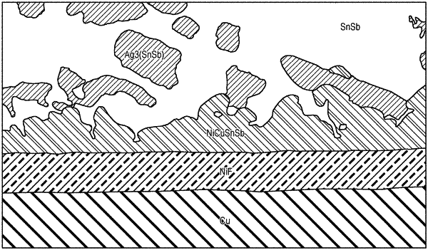
arranging a first solder layer on the first metallization layer, wherein the first solder layer contains the compound Sn/Sb, wherein the material composition of the compound Sn/Sb is such that the ratio of Sb in the compound is in a range from 17% to 90%; and
providing a first contact member comprising a Cu-based base body and a Ni-based layer disposed on a main surface of the Cu-based base body, wherein the first contact member is connected with the Ni-based layer to the first solder layer.
|