| CPC H01L 23/53238 (2013.01) [H01L 21/78 (2013.01); H01L 23/3107 (2013.01); H01L 23/481 (2013.01); H01L 25/0657 (2013.01); H01L 25/50 (2013.01)] | 14 Claims |
|
1. A semiconductor die, comprising:
integrated circuitry at a front side of the semiconductor die;
a dielectric layer at a back side of the semiconductor die opposite to the front side; and
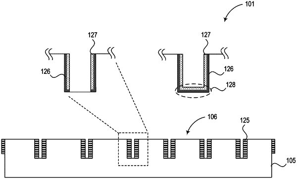
a metallic layer at an outermost sidewall of the semiconductor die, the metallic layer extending from the front side to the back side, wherein the metallic layer surrounds the outermost sidewall such that the metallic layer completely covers the outermost sidewall.
|