| CPC H01L 23/5283 (2013.01) [H01L 21/76832 (2013.01); H01L 21/76843 (2013.01); H01L 23/5226 (2013.01)] | 20 Claims |
|
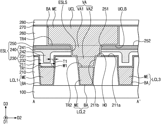
1. A semiconductor device, comprising:
a substrate;
an active pattern on the substrate, the active pattern having an upper portion that protrudes upwardly;
a source/drain pattern on the substrate;
a gate electrode on the substrate;
a lower dielectric layer that covers the source/drain pattern;
a contact that penetrate the lower dielectric layer and is connected to the source/drain pattern;
a first dielectric layer on the lower dielectric layer;
a first lower conductive line in the first dielectric layer and connected to the contact;
an etch stop layer on the first dielectric layer;
a via-structure that penetrates the etch stop layer and is connected to the first lower conductive line; and
an upper conductive line connected to the via-structure,
wherein the first dielectric layer includes a dielectric pattern at a level higher than a top surface of the first lower conductive line, and
wherein the etch stop layer has an upper portion with a rounded surface in contact with the via-structure.
|