| CPC H01L 23/3675 (2013.01) [H01L 21/4882 (2013.01); H01L 28/40 (2013.01); H01L 23/10 (2013.01); H01L 23/42 (2013.01); H01L 24/30 (2013.01); H01L 24/32 (2013.01)] | 20 Claims |
|
1. A device package, comprising:
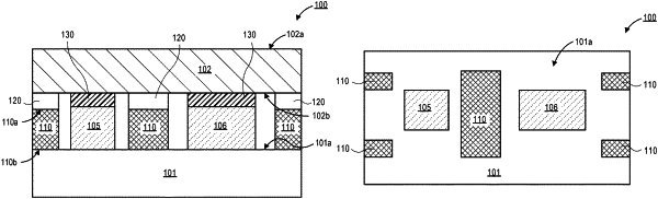
one or more dies disposed on a substrate;
one or more conductive layers disposed on the one or more dies, wherein the one or more conductive layers comprises a first conductive layer laterally adjacent to a second conductive layer on one of the one or more dies, the second conductive layer different than the first conductive layer; and
a lid with one or more legs on an outer periphery of the lid, a top surface, and a bottom surface that is opposite from the top surface, wherein the one or more legs of the lid are attached to the substrate with a sealant, and wherein the bottom surface of the lid is disposed over the one or more conductive layers and the one or more dies on the substrate.
|