| CPC G11C 17/18 (2013.01) [G11C 17/16 (2013.01); G11C 29/08 (2013.01)] | 17 Claims |
|
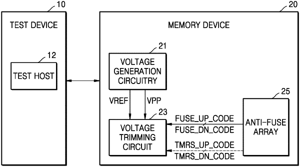
1. A memory device configured to perform a voltage trimming operation, the memory device comprising:
a voltage generation circuit configured to generate a reference voltage and a first voltage;
a voltage trimming circuit configured to trim the reference voltage to the first voltage and to output a voltage detection signal by comparing a voltage level of a reference voltage trimming node determined by a first resistance value of a first resistance circuit and a second resistance value of a second resistance circuit to a voltage level of a feedback node connected to the first voltage; and
a non-volatile storage storing up codes and down codes,
wherein the voltage trimming circuit performs a first voltage trimming during a wafer test of the memory device, and a second voltage trimming during a package test of the memory device,
wherein the first voltage trimming adjusts the up codes and the down codes with respect to the first voltage provided at a target voltage level in response to the voltage detection signal, and
the second voltage trimming adjusts the up codes and the down codes with respect to the first voltage provided with a target voltage level range having a positive or negative range with respect to the target voltage level in response to the voltage detection signal.
|