| US 11,776,639 B2 | ||
| Modified distribution of memory device states | ||
| Amiya Banerjee, Bangalore (IN); Vinayak Bhat, Bangalore (IN); and Harish R. Singidi, Fremont, CA (US) | ||
| Assigned to Western Digital Technologies, Inc., San Jose, CA (US) | ||
| Filed by Western Digital Technologies, Inc., San Jose, CA (US) | ||
| Filed on Oct. 3, 2022, as Appl. No. 17/959,029. | ||
| Application 17/959,029 is a continuation of application No. 17/319,756, filed on May 13, 2021, granted, now 11,462,279, issued on Oct. 4, 2022. | ||
| Prior Publication US 2023/0021663 A1, Jan. 26, 2023 | ||
| Int. Cl. G11C 16/34 (2006.01); G11C 16/26 (2006.01); G11C 16/10 (2006.01) | ||
| CPC G11C 16/3418 (2013.01) [G11C 16/102 (2013.01); G11C 16/26 (2013.01); G11C 16/3404 (2013.01)] | 20 Claims |
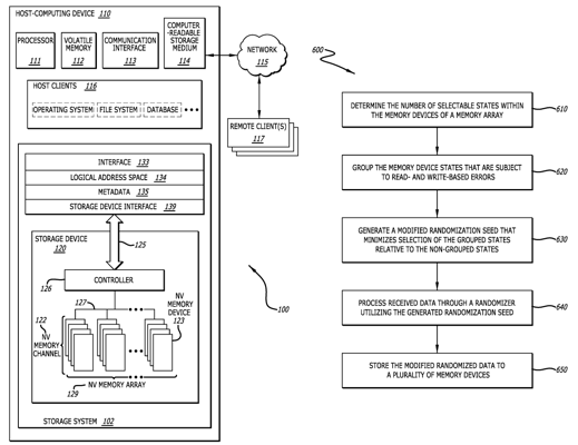
|
1. A device comprising:
a processor; a memory array comprising: a plurality of memory devices configured to be programmed into a plurality of states, each state corresponding to a unique value; a distribution logic configured to:
receive host data for storage;
parse the received host data into a plurality of values suitable for storage;
determine a first portion of the plurality of values having a high read frequency;
determine a first probability for storing the first portion of the plurality of values within a first portion of the plurality of memory devices;
determine a second probability for storing a remaining portion of the plurality of values within a second portion of the plurality of memory devices;
store each of the first portion of the plurality of values within one of a first plurality of states in the first portion of the plurality of memory devices; and
store each of the second portion of the plurality of values within one of a second plurality of states in the second portion of the plurality of memory devices.
|