| CPC G11C 11/4093 (2013.01) [G11C 11/408 (2013.01); G11C 11/4096 (2013.01); H10B 12/00 (2023.02); G11C 29/02 (2013.01)] | 20 Claims |
|
1. An apparatus comprising:
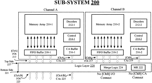
a mode register to indicate a mode of operation for a high bandwidth memory stack device to include a plurality of memory devices stacked above a logic layer; and
circuitry at the logic layer to execute logic, the logic to:
read a value of the mode register; and
cause, based on the value of the mode register, a portion of input/output (I/O) contacts on a bottom side of the logic layer to be inactive and a remaining portion of the I/O contacts to be active, the portion of I/O contacts arranged to receive or transmit I/O signals for one or more data channels to access the plurality of memory devices.
|