| CPC G09G 3/3266 (2013.01) [G11C 19/28 (2013.01); G09G 2300/0426 (2013.01); G09G 2310/0286 (2013.01)] | 20 Claims |
|
1. A display substrate, comprising:
a base substrate, comprising a display region and a peripheral region on at least one side of the display region; and
a shift register unit, a first clock signal line, and a second clock signal line, which are on the peripheral region of the base substrate,
wherein the first clock signal line and the second clock signal line extend along a first direction on the base substrate, and are configured to respectively provide a first clock signal and a second clock signal to the shift register unit,
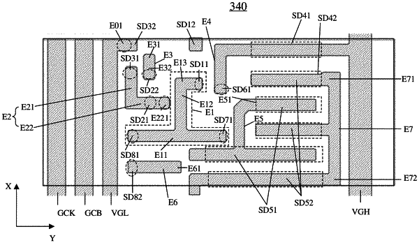
wherein the shift register unit comprises an input circuit, an output circuit, a first control circuit, a second control circuit, and a voltage stabilizing circuit,
wherein the input circuit is configured to input an input signal to a first node in response to the first clock signal,
wherein the first control circuit is connected to the first node and a second node, and is configured to control a level of the second node in response to a level of the first node and the first clock signal,
wherein the second control circuit is connected to the first node and the second node, and is configured to control the level of the first node under control of the level of the second node and the second clock signal,
wherein the voltage stabilizing circuit is connected to the first node and a third node, and is configured to stabilize a level of the third node,
wherein the output circuit is connected to the third node, and is configured to output an output signal to an output terminal under control of the level of the third node,
wherein the first control circuit comprises a first control transistor, the second control circuit comprises a first noise reduction transistor, the voltage stabilizing circuit comprises a voltage stabilizing transistor, a gate electrode of the first control transistor, a first electrode of the first noise reduction transistor, and a first electrode of the voltage stabilizing transistor are all connected to the first node,
wherein the first electrode of the first noise reduction transistor and the first electrode of the voltage stabilizing transistor are in a first source-drain electrode layer, and the first source-drain electrode layer comprises a first transfer electrode, and
wherein the first transfer electrode comprises a first portion extending in parallel along a second direction different from the first direction and a second portion integrally formed with the first portion and extending along the first direction, a first end of the first portion is connected to the first electrode of the first noise reduction transistor, a second end of the first portion is connected to the first electrode of the voltage stabilizing transistor, and the second portion is connected to the gate electrode of the first control transistor that is not in a same layer as the second portion.
|