| CPC G09G 3/3225 (2013.01) [G11C 19/28 (2013.01); G09G 2300/0852 (2013.01); G09G 2310/0286 (2013.01)] | 16 Claims |
|
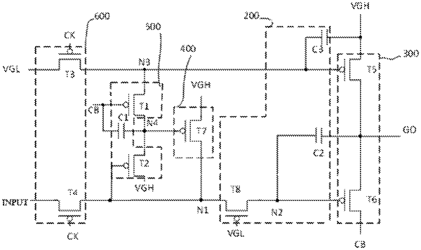
1. A shift register unit, comprising a first input circuit, a second input circuit, a control circuit and an output circuit, wherein
the first input circuit is respectively coupled to an input terminal, a second voltage terminal, a second clock signal terminal, a first node and a third node, and is configured to provide an input signal to the first node and provide a second voltage signal to the third node in response to a second clock signal provided by the second clock signal terminal; the input terminal is configured to provide the input signal, and the second voltage terminal is configured to provide the second voltage signal;
the second input circuit is respectively coupled to an input control terminal, the first node, the third node, a fourth node and a first voltage terminal, and is configured to output a first voltage signal to the third node and control a potential at the fourth node in response to a potential at the first node and an input control signal provided by the input control terminal; the input control terminal is a first clock signal terminal or a third clock signal terminal, and the input control signal is a first clock signal provided by the first clock signal terminal or a clock signal provided by the third clock signal terminal;
the control circuit is respectively coupled to the first node, the fourth node and the first voltage terminal and is configured to provide the first voltage signal to the first node in response to the potential at the fourth node; the first voltage terminal is configured to provide the first voltage signal; and
the output circuit is electrically coupled to the third node, the first node, the first voltage terminal, the first clock signal terminal and an output terminal, respectively, and is configured to control a signal output by the output terminal according to a potential at the third node, a potential at the first node, the first voltage signal and the first clock signal.
|