| CPC G09G 3/2092 (2013.01) [G09G 3/3258 (2013.01); G09G 3/3291 (2013.01); G09G 2310/061 (2013.01)] | 13 Claims |
|
1. A display substrate, comprising a substrate, a light shielding layer, an active layer, a first gate layer, a source-drain layer and a second gate layer, wherein the display substrate further comprises a plurality of pixel units disposed in an array, wherein each of the plurality of pixel units comprises a pixel circuit, and the pixel circuit comprises a light-emitting element, a voltage providing module, a voltage writing-in module and a driving module; wherein
the voltage providing module is respectively connected with a first power supply voltage terminal, an initial voltage terminal, a reset signal terminal, a light-emitting control terminal, the voltage writing-in module and the driving module, and the voltage providing module is configured to provide a voltage of the first power supply voltage terminal and a voltage of the initial voltage terminal to the driving module under control of the reset signal terminal to turn on the driving module; and provide the voltage of the first power supply voltage terminal to the driving module under control of the light-emitting control terminal;
the voltage writing-in module is respectively connected with a signal terminal, a data input terminal, the initial voltage terminal, the voltage providing module, the driving module and the light-emitting element, and the voltage writing-in module is configured to write a data voltage into the driving module under control of the signal terminal;
the driving module is respectively connected with the voltage providing module and the voltage writing-in module, the driving module is separate from the voltage writing-in module, and the driving module is configured to provide a driving current to the light-emitting element, and
the first gate layer is connected with the light-emitting element, and the second gate layer is located above the first gate layer;
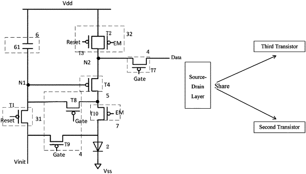
wherein the voltage providing module comprises a voltage supply module, the voltage supply module comprises a second transistor and a third transistor, and the second transistor and the third transistor share a source-drain layer.
|