| CPC G09G 3/2007 (2013.01) [G09G 3/32 (2013.01); G09G 2300/0408 (2013.01); G09G 2300/0819 (2013.01); G09G 2310/0286 (2013.01); G09G 2320/066 (2013.01)] | 19 Claims |
|
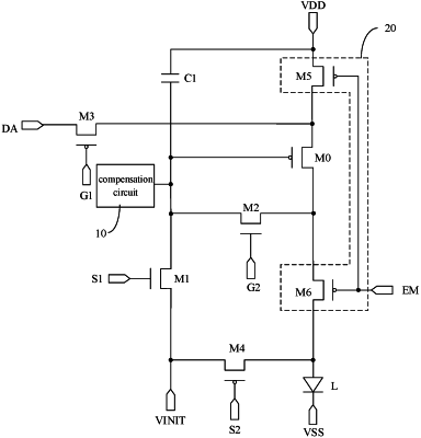
1. A pixel circuit, comprising:
a data writing transistor, wherein a gate of the data writing transistor is electrically connected with a first scan line, a first electrode of the data writing transistor is electrically connected with a data line, a second electrode of the data writing transistor is electrically connected with a first electrode of a drive transistor; wherein a material of an active layer of the data writing transistor is a low temperature poly-silicon material;
a threshold compensation transistor, wherein a gate of the threshold compensation transistor is electrically connected with a second scan line, a first electrode of the threshold compensation transistor is electrically connected with a gate of the drive transistor, a second electrode of the threshold compensation transistor is electrically connected with a second electrode of the drive transistor; wherein a material of an active layer of the threshold compensation transistor is a metal oxide semiconductor material;
a compensation circuit, electrically connected with the gate of the drive transistor and configured to compensate for a voltage of the gate of the drive transistor according to a parasitic capacitor; and
a light emitting control circuit, electrically connected with a first power end, the first electrode and the second electrode of the drive transistor and a first electrode of a light emitting device, and configured to turn on the first power end and the first electrode of the drive transistor and turn on the second electrode of the drive transistor and the first electrode of the light emitting device under control of a signal of a light emitting control line to drive the light emitting device to emit light;
wherein the parasitic capacitor is a channel capacitor between the gate and the first electrode of the threshold compensation transistor; and
a capacitance value of the channel capacitor between the gate and the first electrode of the threshold compensation transistor is a first channel capacitance value, and a difference between a capacitance value of the compensation circuit and the first channel capacitance value is substantially 0.
|