| CPC G09G 3/20 (2013.01) [G09G 2300/0408 (2013.01); G09G 2310/0267 (2013.01); G09G 2310/08 (2013.01); G09G 2330/021 (2013.01)] | 10 Claims |
|
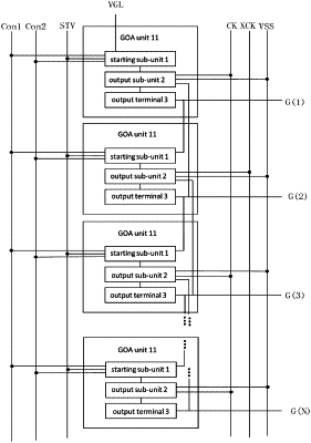
1. A gate driving circuit for driving a pixel array, and the gate driving circuit comprises a plurality of Gate Driver On Array (GOA) units which are cascaded, each of the GOA units drives a row of pixels, each of the GOA units comprises a starting sub-unit, an output sub-unit and an output terminal which are coupled in sequence, wherein,
the starting sub-unit of the GOA unit at a first stage is coupled with a starting signal, a first control signal, a second control signal and a constant voltage potential respectively, and the output sub-unit of the GOA unit at the first stage is coupled with a first clock signal and a first power supply signal respectively;
the starting sub-unit of the GOA unit at an nth stage is coupled with the starting signal, the first control signal, the second control signal and the output terminal of the GOA unit at an (n−1)th stage respectively, the output sub-unit of the GOA unit at the nth stage is coupled with the first power supply signal and the output terminal of the GOA unit an (n+1)th stage, wherein n is an integer greater than 1, and in response to that n is an odd number, the output sub-unit of the GOA unit at the nth stage is further coupled with the first clock signal, and in response to that n is an even number, the output sub-unit of the GOA unit at the nth stage is further coupled with the second clock signal,
the gate driving circuit starts or stops scanning a corresponding row of pixels of the pixel array according to the first control signal, the second control signal and the starting signal,
wherein the output sub-unit of the GOA unit at each stage comprises:
a first thin film transistor, a gate electrode and a source electrode of the first thin film transistor are coupled to each other;
a second thin film transistor, a gate electrode of the second thin film transistor is coupled to a drain electrode of the first thin film transistor to form a first node, a source electrode of the second thin film transistor is coupled to the first clock signal or the second clock signal, and a drain electrode of the second thin film transistor is coupled to an output terminal of the GOA unit at a current stage;
a third thin film transistor, a gate electrode of the third thin film transistor is coupled to the output terminal of the GOA unit at a next stage, a source electrode of the third thin film transistor is coupled to the first node, and a drain electrode of the third thin film transistor is coupled with the first power supply signal; and
a fourth thin film transistor, a gate electrode of the fourth thin film transistor is coupled to the output terminal of the GOA unit at the next stage, a source electrode of the fourth thin film transistor is coupled to the drain electrode of the second thin film transistor, and a drain electrode of the fourth thin film transistor is coupled with the first power supply signal.
|