| CPC G09G 3/006 (2013.01) [G09G 3/3233 (2013.01); G09G 2300/0842 (2013.01); G09G 2320/0233 (2013.01); G09G 2320/0295 (2013.01); G09G 2320/045 (2013.01); G09G 2360/16 (2013.01)] | 20 Claims |
|
1. A detecting method of a pixel circuit, wherein the pixel circuit comprises a driving transistor, and the detecting method comprises:
in a first charging cycle, applying a first data voltage to a gate electrode of the driving transistor, and in a first time duration after applying the first data voltage and before the driving transistor is turned off, obtaining a first sensing voltage at a first electrode of the driving transistor and determining whether the first sensing voltage is equal to a first reference sensing voltage; and
in a second charging cycle, applying a second data voltage to the gate electrode of the driving transistor, and in a second time duration after applying the second data voltage and before the driving transistor is turned off, obtaining a second sensing voltage at the first electrode of the driving transistor and determining whether the second sensing voltage is equal to a second reference sensing voltage;
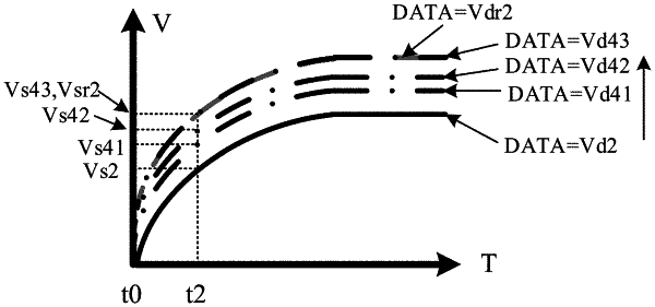
wherein if the first sensing voltage is equal to the first reference sensing voltage and the second sensing voltage is equal to the second reference sensing voltage, obtaining a present current coefficient of the driving transistor according to the first data voltage, the second data voltage and a first formula: K=(Vd1−Vd2)/(L11/2−L21/2); and obtaining a present threshold voltage of the driving transistor according to a second formula: Vth=(Vd2*L11/2−Vd1*L21/2)/(L11/2−L21/2);
wherein K represents the present current coefficient of the driving transistor, Vth represents the present threshold voltage of the driving transistor, Vd1 represents the first data voltage, Vd2 represents the second data voltage, L1 represents a first luminance value, L2 represents a second luminance value, and the first luminance value and the second luminance value are both specified normalized luminance values.
|