US 11,775,722 B2
Systems and methods for obfuscating a circuit design
Bertrand Irissou, San Jose, CA (US); John M. Hughes, Hartford, CT (US); Lucio Lanza, Palo Alto, CA (US); Mohamed K. Kassem, Carlsbad, CA (US); Michael S. Wishart, Hillsborough, CA (US); Rajeev Srivastava, Austin, TX (US); Risto Bell, San Jose, CA (US); Robert Timothy Edwards, Poolesville, MD (US); Sherif Eid, Sunnyvale, CA (US); and Greg P. Shaurette, Tahoe City, CA (US)
Assigned to efabless corporation, San Jose, CA (US)
Filed by efabless corporation, San Jose, CA (US)
Filed on Oct. 4, 2021, as Appl. No. 17/493,576.
Application 17/493,576 is a continuation of application No. 16/879,045, filed on May 20, 2020, granted, now 11,301,609.
Application 16/879,045 is a continuation of application No. 16/564,536, filed on Sep. 9, 2019, granted, now 10,671,700, issued on Jun. 2, 2020.
Application 16/564,536 is a continuation of application No. 15/633,412, filed on Jun. 26, 2017, granted, now 10,423,748, issued on Sep. 24, 2019.
Claims priority of provisional application 62/359,858, filed on Jul. 8, 2016.
Prior Publication US 2022/0027544 A1, Jan. 27, 2022
Int. Cl. G06F 30/39 (2020.01); G06F 30/30 (2020.01); G06F 30/33 (2020.01); G06F 30/367 (2020.01); G06F 30/392 (2020.01); G06F 30/398 (2020.01); G06F 30/3323 (2020.01); H01L 23/00 (2006.01); G06F 119/18 (2020.01)
CPC G06F 30/39 (2020.01) [G06F 30/30 (2020.01); G06F 30/33 (2020.01); G06F 30/3323 (2020.01); G06F 30/367 (2020.01); G06F 30/392 (2020.01); G06F 30/398 (2020.01); H01L 23/573 (2013.01); G06F 2119/18 (2020.01)] 22 Claims
OG exemplary drawing
 
1. A method for generating an integrated circuit (IC) chip design, comprising:
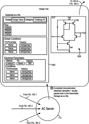
receiving, by a server, a plurality of electrical parameters of a system on chip (SoC) to be designed, wherein the plurality of electrical parameters are received on a data sheet;
receiving a plurality of physical parameters of the SoC on the data sheet;
generating a first design of the SoC according to the plurality of electrical parameters and the plurality of physical parameters;
receiving a plurality of test parameters for testing the first design;
testing, via a design verification tool, the first design by applying the plurality of test parameters to the first design;
receiving a second design of a second SoC;
coupling the second design to the first design to generate a first IC chip design; and
arranging the first IC chip design to be included on a shuttle for fabricating a first IC chip.