| CPC G06F 12/08 (2013.01) [G06N 3/063 (2013.01); G11C 11/418 (2013.01); G11C 11/419 (2013.01)] | 16 Claims |
|
1. An integrated circuit, comprising:
a first port and a second port; and
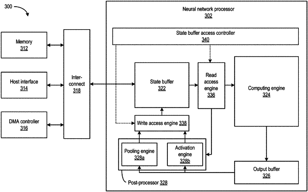
a read access engine configured to:
receive, from a first access requester device, a first read request to fetch first data stored at a memory device;
receive, from a second access requester device, a second read request to fetch second data stored at the memory device;
provide, via the first port, a sequential access of a plurality of portions of the first data to the first access requester device by:
receiving the plurality of portions of the first data from the memory device during a first single clock cycle and outputting the plurality of portions of the first data to the first access requester device during multiple clock cycles;
provide, via the second port, a sequential access of a plurality of portions of the second data to the second access requester device by:
receiving the plurality of portions of the second data from the memory device during a second single clock cycle and outputting the plurality of portions of the second data to the first access requester device during the multiple clock cycles, wherein the second single clock cycle is after the first single clock cycle, and wherein the multiple clock cycles are after the second single clock cycle.
|