| CPC G06F 9/4498 (2018.02) [G05B 11/01 (2013.01); G05B 19/045 (2013.01); G06F 3/0604 (2013.01); G06F 3/0653 (2013.01); G06F 7/00 (2013.01)] | 20 Claims |
|
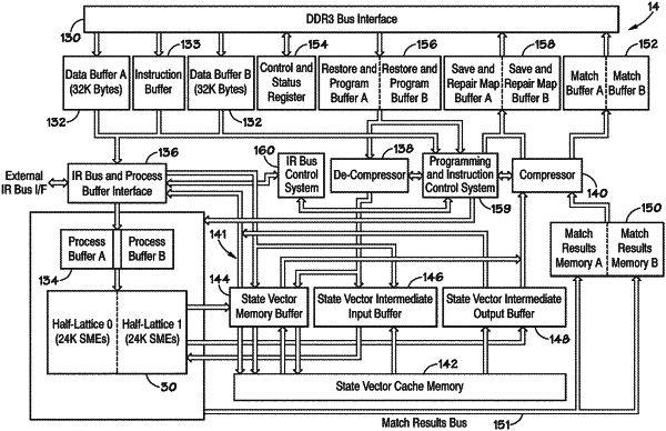
1. An apparatus, comprising:
a primary chip configured to initiate a first write operation at a first clock rate; and
a secondary chip coupled to the primary chip and configured to receive first data from the primary chip at the first clock rate as part of the first write operation, wherein the primary chip comprises a bus control system configured to receive an indication of an amount of data locations being utilized in a storage location of the primary chip and transmit a halt signal configured to halt the first write operation based, at least in part, on the amount of data locations being utilized in the storage location.
|
|
14. An apparatus, comprising:
a primary chip comprising a first storage location, wherein the primary chip is configured to initiate a write operation at a first clock rate; and
a secondary chip coupled to the primary chip and configured to receive first data from the primary chip at the first clock rate as part of the write operation, wherein the primary chip comprises a bus control system configured to:
receive an indication of an amount of data locations being utilized in the first storage location;
determine if any of the data locations in the first storage location are available;
transmit an indication to allow writing of additional data to the available data locations at the first write clock speed prior to halting the write operation when the bus control system determines that the available data locations are available; and
transmit a halt signal configured to halt the write operation when the available data locations have been filled.
|
|
18. A method, comprising:
initiating a write operation by a primary chip;
transmitting first data from the primary chip to a secondary chip as part of the write operation;
determining an overflow indication as in an indication of an amount of data locations being utilized in a storage location of the primary chip; and
transmitting a halt signal configured to halt the write operation based, at least in part, on the amount of data locations being utilized in the storage location.
|