US 11,775,208 B2
Partitions within snapshot memory for buffer and snapshot memory
Kishore K. Muchherla, Fremont, CA (US); Niccolo′ Righetti, Boise, ID (US); Jeffrey S. McNeil, Jr., Nampa, ID (US); Akira Goda, Boise, ID (US); Todd A. Marquart, Boise, ID (US); Mark A. Helm, Santa Cruz, CA (US); Gil Golov, Backnang (DE); Jeremy Binfet, Boise, ID (US); Carmine Miccoli, Boise, ID (US); and Giuseppina Puzzilli, Boise, ID (US)
Assigned to Micron Technology, Inc., Boise, ID (US)
Filed by Micron Technology, Inc., Boise, ID (US)
Filed on Jun. 1, 2022, as Appl. No. 17/829,861.
Application 17/829,861 is a continuation of application No. 16/995,645, filed on Aug. 17, 2020, granted, now 11,360,700.
Prior Publication US 2022/0291865 A1, Sep. 15, 2022
This patent is subject to a terminal disclaimer.
Int. Cl. G06F 3/06 (2006.01); G06F 1/26 (2006.01)
CPC G06F 3/0656 (2013.01) [G06F 1/263 (2013.01); G06F 3/0613 (2013.01); G06F 3/0619 (2013.01); G06F 3/0644 (2013.01); G06F 3/0653 (2013.01); G06F 3/0673 (2013.01)] 20 Claims
OG exemplary drawing
 
1. A system, comprising:
a processing device; and
a memory device communicatively coupled to the processing device and comprising:
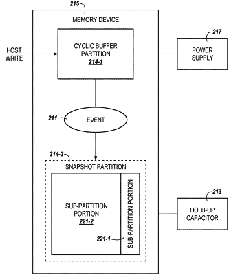
a cyclic buffer portion; and
a snapshot portion coupled to the cyclic buffer portion, the snapshot portion further comprising:
a first portion having a first programming characteristic; and
a second portion having a second programming characteristic;
wherein the processing device is to:
write received data sequentially to the first portion; and
write, based at least in part on a determination that a trigger event has occurred, data from the cyclic buffer to the first or second portion of the snapshot portion, or both.