US 11,775,124 B2
Display device and method of driving the same in two modes
Kangwon Lee, Seoul (KR); Incheol Kim, Goyang-si (KR); Ung Choi, Anyang-si (KR); Won-Ki Hong, Suwon-si (KR); Seungho Nam, Seongnam-si (KR); Jihong Park, Suwon-si (KR); Chul Kim, Hwaseong-si (KR); Hojin Byun, Suwon-si (KR); and Kiseok Cha, Yongin-si (KR)
Assigned to Samsung Display Co., Ltd., Yongin-si (KR)
Filed by Samsung Display Co., Ltd., Yongin-si (KR)
Filed on Apr. 3, 2022, as Appl. No. 17/712,170.
Application 17/152,722 is a division of application No. 16/163,301, filed on Oct. 17, 2018, granted, now 10,921,924, issued on Feb. 16, 2021.
Application 16/163,301 is a division of application No. 15/179,315, filed on Jun. 10, 2016, granted, now 10,191,580, issued on Jan. 29, 2019.
Application 15/179,315 is a division of application No. 14/024,241, filed on Sep. 11, 2013, granted, now 9,389,737, issued on Jul. 12, 2016.
Application 17/712,170 is a continuation of application No. 17/152,722, filed on Jan. 19, 2021, granted, now 11,314,368.
Claims priority of provisional application 61/701,100, filed on Sep. 14, 2012.
Claims priority of application No. 10-2013-0021423 (KR), filed on Feb. 27, 2013; application No. 10-2013-0021426 (KR), filed on Feb. 27, 2013; and application No. 10-2013-0055845 (KR), filed on May 16, 2013.
Prior Publication US 2022/0221958 A1, Jul. 14, 2022
This patent is subject to a terminal disclaimer.
Int. Cl. G06F 3/041 (2006.01); G06F 3/044 (2006.01); G09G 3/20 (2006.01)
CPC G06F 3/0446 (2019.05) [G06F 3/044 (2013.01); G06F 3/0412 (2013.01); G06F 3/0416 (2013.01); G06F 3/0445 (2019.05); G09G 3/20 (2013.01); G06F 2203/04106 (2013.01); G09G 2300/023 (2013.01)] 14 Claims
OG exemplary drawing
 
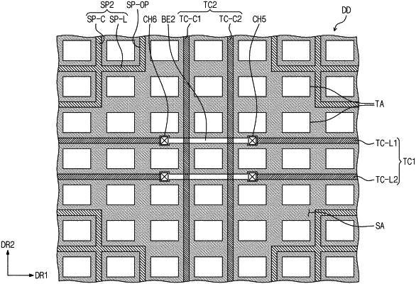
1. A display device, comprising:
a display panel including a black matrix having a plurality of openings; and
a touch panel on the display panel, the touch panel comprising:
a first electrode including first sensor parts and first connection parts, each of the first connection parts connecting two adjacent first sensor parts among the first sensor parts;
a second electrode crossing the first electrode and including second sensor parts and second connection parts, each of the second connection parts connecting two adjacent second sensor parts among the second sensor parts;
a first electromagnetic inducing electrode; and
a second electromagnetic inducing electrode crossing the first electromagnetic inducing electrode,
wherein a crossing area of the first electromagnetic inducing electrode and second electromagnetic inducing electrode overlaps a corresponding sensor part among the first sensor parts and the second sensor parts, and
wherein the first electromagnetic inducing electrode and the second electromagnetic inducing electrode overlap the black matrix without overlapping the openings.