| CPC G06F 3/04166 (2019.05) [G06F 3/0412 (2013.01); H10K 59/131 (2023.02); H10K 59/40 (2023.02); G06F 2203/04107 (2013.01)] | 20 Claims |
|
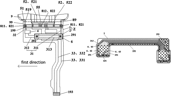
1. A display apparatus, comprising a display panel and a circuit board assembly, wherein the circuit board assembly comprises a main circuit board and a jumper connection circuit board;
the display panel comprises a substrate, a display structure arranged on the substrate and a touch control structure arranged on a side of the display structure away from the substrate; the display panel has a first bonding region, and a plurality of first display terminals electrically coupled with the display structure and a plurality of first touch control terminals electrically coupled with the touch control structure are arranged in the first bonding region;
the display panel comprises a panel chip;
the main circuit board has a second bonding region, a connection region, a first region and a second region; the second bonding region is bonded with the first bonding region, and a plurality of second display terminals electrically coupled with the first display terminals respectively and a plurality of second touch control terminals electrically coupled with the first touch control terminals respectively are arranged in the second bonding region; a plurality of main connectors are respectively arranged in the first region and the second region;
the main circuit board comprises a touch control chip, a plurality of display lines and a plurality of segment touch control lines; each of the segment touch control lines comprises a first segment and a second segment, wherein the first segment is coupled between one of the second touch control terminals and one of the main connectors in the first region, and the second segment is coupled between the touch control chip and one of the main connectors in the second region; at least a portion of the display lines are coupled between the second display terminals and the connection region and are crossed with a line connected between the first region and the second region;
the jumper connection circuit board has a third region and a fourth region;
the third region is bonded with the first region, and the fourth region is bonded with the second region; a plurality of jumper connectors electrically coupled with the main connectors in the first region respectively are arranged in the third region, and a plurality of jumper connectors electrically coupled with the main connectors in the second region respectively are arranged in the fourth region;
the jumper connection circuit board comprises a plurality of jumper connection lines which correspond to the segment touch control lines one by one; each jumper connection line is coupled between one of the jumper connectors in the third region and one of the jumper connectors in the fourth region, and two of the main connectors electrically coupled with such two jumper connectors are respectively coupled with the first segment and the second segment of one of the segment touch control lines;
the main circuit board is a flexible circuit board; the jumper connection circuit board is a flexible circuit board.
|