| CPC G06F 3/04164 (2019.05) [G06F 3/0412 (2013.01); G06F 2203/04103 (2013.01)] | 14 Claims |
|
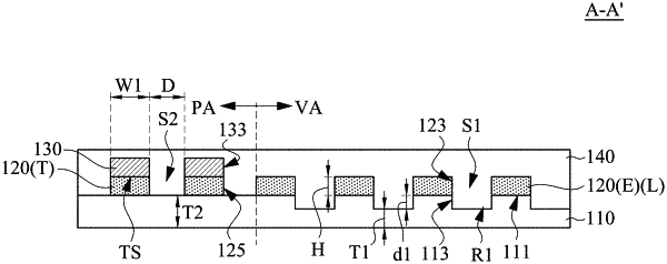
1. A touch sensor having a visible area and a peripheral area adjacent to at least one side of the visible area, the touch sensor comprising:
a substrate comprising a main surface and a secondary surface opposite to the main surface;
a metal nanowire layer disposed on the main surface of the substrate on a side of the main surface facing away from the secondary surface, wherein the metal nanowire layer defines a plurality of electrode portions corresponding to the visible area and defines a plurality of wiring portions corresponding to the peripheral area, the electrode portions are arranged at intervals, the wiring portions are respectively connected to the electrode portions and arranged at intervals, two adjacent electrode portions of the electrode portions are spaced apart by a first spacer region, and two adjacent wiring portions of the wiring portions are spaced apart by a second spacer region; and
a silver layer disposed on the wiring portions and being in contact with the wiring portions;
wherein a thickness of the substrate that corresponds to the first spacer region is smaller than a thickness of the substrate that corresponds to the second spacer region and each thickness is measured from the main surface to the secondary surface in a direction perpendicular to the main surface.
|