| CPC G06F 3/015 (2013.01) [A61B 5/25 (2021.01); G06F 3/0416 (2013.01); G06F 3/0421 (2013.01); G06V 40/1318 (2022.01)] | 12 Claims |
|
1. An image display device comprising:
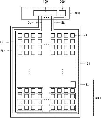
a display panel including a plurality of pixels and a photoresistor pattern formed in a non-light emitting area between adjacent pixels among the plurality of pixels;
a panel driving controller configured to drive gate and data lines, and light-emission control lines of the display panel; and
a bio-signal detector configured to detect an output voltage of the photoresistor pattern during an image display operation and detect a bio-signal of the target object, based on the detected output voltage,
wherein a resistance value of the photoresistor pattern varies based on intensity of light reflected from a target object during the image display operation, and
wherein the photoresistor pattern is formed in a single continuous line shape that is variously bent in the vertical and horizontal directions along the non-light emitting area among the plurality of pixels, and
wherein the photoresistor pattern is separated with and completely overlaps with a switching transistor between adjacent pixels among the plurality of pixels.
|