| CPC G06F 1/12 (2013.01) [G06F 1/08 (2013.01); H03L 7/085 (2013.01)] | 8 Claims |
|
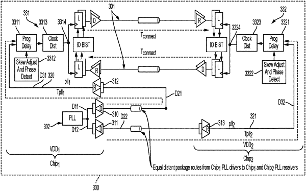
1. A computer-implemented method of clock calibration for each of a first chip and a second chip of a two-chip die module, the first chip comprising a clock distribution unit to generate an output for a clock sample point of the first chip and the second chip comprising a clock distribution unit to generate an output for a clock sample point of the second chip, the method comprising:
arranging layouts of the first and second chips to provide equal delays between a skew adjust and phase detect unit of the second chip and the clock sample points of each of the first and second chips;
setting a voltage signal to a prescribed value for each of the first and second chips;
programming each of the first and second chips for minimal chip switching activity;
setting a programmable delay to a predefined value for each of the first and second chips;
starting clocks on each of the first and second chips and measuring a skew of the second chip from a comparison of relative edge positions of the clock of each of the first and second chips;
incrementally adjusting a latency of the second chip until the skew of each of the first and second chips shows phase alignment of the clock of each of the first and second chips; and
storing the skew of the second chip as a setting once the phase alignment is achieved.
|