| CPC G05F 3/262 (2013.01) | 12 Claims |
|
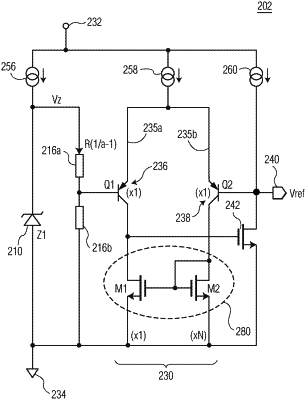
1. An apparatus comprising:
a Zener diode circuit, coupled between a first supply terminal and a second supply terminal, to provide a first input reference voltage level;
a voltage reduction circuit, arranged in parallel with the Zener diode circuit, to provide a second input reference voltage level that tracks the first input reference voltage level; and
a proportional-to-absolute temperature (PTAT) circuit includes a differential circuit having first and second differential paths to provide an output drive current and an output reference voltage at an output node of the PTAT circuit, having a feedforward path to the output node based on the second input reference voltage level, wherein:
the first differential path includes a first transistor circuit to pass current between the first supply terminal and the second supply terminal, the first transistor circuit having a control terminal driven in response to the second input reference voltage level,
the second differential path includes a second transistor circuit to pass current between the first supply terminal and the second supply terminal, the second transistor circuit having a control terminal driven in response to the output reference voltage at the output node, and
the PTAT circuit is configured to provide a level of temperature compensation that is set by a ratio of current density of the first transistor circuit and the second transistor circuit.
|