| CPC G02F 1/1368 (2013.01) [G02F 1/136209 (2013.01); G02F 1/136286 (2013.01); G09G 3/3677 (2013.01)] | 16 Claims |
|
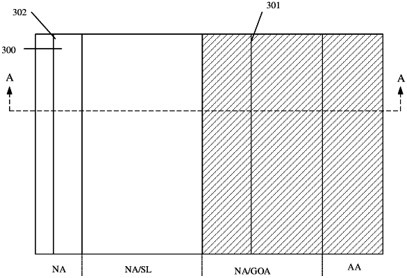
1. A display panel having a display area and a peripheral area surrounding the display area, the display panel comprising an array substrate, an opposite substrate and a sealant layer between the array substrate and the opposite substrate to seal a periphery of the array substrate and a periphery of the opposite substrate, wherein
the sealant layer is arranged in the peripheral area, and the sealant layer has a first edge close to the display area and a second edge away from the display area,
the array substrate comprises a base substrate, a driving circuit arranged on the base substrate, and an organic insulating layer arranged at a side of the driving circuit away from the base substrate,
the organic insulating layer comprises a first part and a second part, wherein the first part overlaps with the sealant layer in a direction perpendicular to a substrate surface of the base substrate, the second part has no overlap with the sealant layer, and an edge of the first part away from the display area is located between the first edge and the second edge in a direction parallel to the substrate surface of the base substrate, and
the driving circuit comprises a gate scan driving circuit arranged in the peripheral area, and the gate scan driving circuit at least partially overlaps with the first part in the direction perpendicular to the substrate surface of the base substrate,
the gate scan driving circuit comprises a plurality of active devices, and orthographic projections of the plurality of active devices on a plane of the organic insulating layer is located inside the organic insulating layer,
in the direction perpendicular to the substrate surface of the base substrate, the first part comprises an organic insulating pattern overlapped with the plurality of active devices of the gate scan driving circuit and a hollow portion having no overlap with the plurality of active devices of the gate scan driving circuit,
the organic insulating pattern overlapped with the plurality of active devices of the gate scan driving circuit comprises a plurality of portions spaced apart from each other, and the plurality of portions overlap with the plurality of active devices, in a one-to-one correspondence, in the direction perpendicular to the substrate surface of the base substrate, and
the plurality of active devices comprise a plurality of thin film transistors, and the plurality of thin film transistors comprise a plurality of active layers, and orthographic projections of the plurality of active layers on the base substrate are located within orthographic projections of the plurality of portions on the base substrate.
|