| CPC G02F 1/136286 (2013.01) [G02F 1/1368 (2013.01)] | 18 Claims |
|
1. A display substrate, comprising:
a base substrate, the base substrate comprising a display region and a peripheral region surrounding the display region, wherein at least one bonding element configured to be electrically connected to an external component is disposed in the peripheral region, the bonding element comprises a first conductive layer, and the first conductive layer comprises a metal oxide conductive lead;
the bonding element further comprises a second conductive layer located between the first conductive layer and the base substrate, and the second conductive layer comprises a metal conductive lead;
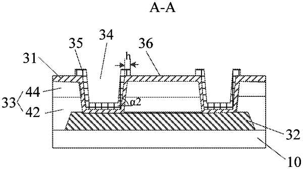
the bonding element further comprises an insulation layer located between the second conductive layer and the first conductive layer, wherein a plurality of via holes are provided in a region of the insulation layer corresponding to at least one metal oxide conductive lead, the at least one metal oxide conductive lead comprises a part located on the insulation layer in contact with the insulation layer and a part extending into the via hole in the insulation layer;
the metal conductive lead and the metal oxide conductive lead are connected in one-to-one correspondence, and the metal conductive lead is electrically connected to the metal oxide conductive lead through the plurality of via holes;
the bonding element further comprises a via hole protection layer disposed on a region of the metal oxide conductive lead corresponding to the via holes,
wherein in a same bonding element, an area of an orthographic projection of the via hole protection layer on the base substrate is less than an area of an orthographic projection of a surface, which is not covered by the via hole protection layer and is between adjacent via holes provided with the via hole protection layer, of the first conductive layer on the base substrate; and
wherein the via hole protection layer comprises at least one metal layer, the display substrate further comprises a reflection electrode located in the display region, a material of the reflection electrode is the same as a material of the at least one metal layer, and the via hole protection layer disposed in a same layer as the reflection electrode.
|