| CPC G02B 30/31 (2020.01) [G02F 1/13306 (2013.01); G02F 1/13439 (2013.01); G02F 1/133553 (2013.01); G02F 1/167 (2013.01); G02F 1/1677 (2019.01); H04N 13/31 (2018.05); H10K 59/50 (2023.02)] | 20 Claims |
|
1. A display substrate, comprising: a light emitting substrate and a grating substrate comprising: a first base substrate and a plurality of grating units on the first base substrate,
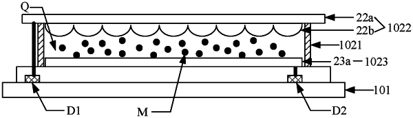
wherein each of the grating units comprises two control layers, a barrier structure between the two control layers, and a plurality of movable particles in a closed cavity surrounded by the barrier structure and the two control layers, wherein the two control layers comprise a first control layer and a second control layer, the first control layer being located on a side of the second control layer distal from the first base substrate, and the two control layers being configured to control movement of the particles;
wherein the particles have a refractive index smaller than a refractive index of the first control layer, and the particles are non-transparent particles; and
the first control layer in each of the grating units comprises a first transparent electrode and a reflective film that are stacked, the reflective film being located on a side of the first transparent electrode proximal to the first base substrate, the second control layer in each of the grating units comprises a second transparent electrode, the particles are charged particles, wherein the charged particles have a refractive index smaller than a refractive index of the reflective film, such that the particles in the closed cavity are moved to a surface of the reflective film proximal to the second control layer by applying a first voltage between the first transparent electrode and the second transparent electrode, to inhibit each of the grating units from transmitting light; and
wherein the light emitting substrate comprises a second base substrate and a plurality of light emitting units on the second base substrate, the light emitting substrate and the grating substrate are oppositely arranged, and the light emitting units are arranged in one-to-one correspondence with the grating units in the grating substrate.
|