| CPC G02B 6/2934 (2013.01) [G01J 1/0425 (2013.01); G01J 1/44 (2013.01); G02B 6/12007 (2013.01); G02F 1/2257 (2013.01); H01L 31/02327 (2013.01); H01L 31/105 (2013.01); G01J 2001/446 (2013.01); G02B 6/29338 (2013.01); G02F 2203/15 (2013.01)] | 19 Claims |
|
1. A photodetector system, comprising:
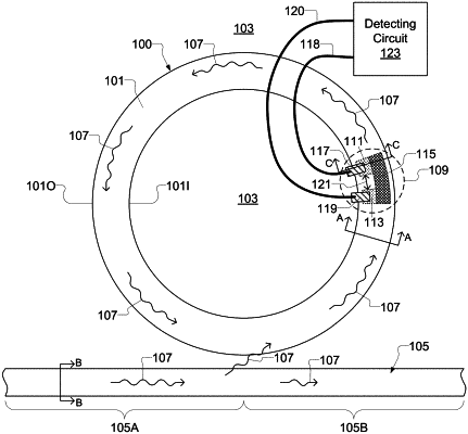
a ring resonator device having a passive optical cavity;
a photodetector device built into the passive optical cavity of the ring resonator;
a tap-off optical waveguide positioned next to the passive optical cavity of the ring resonator device such that some light will evanescently couple from the passive optical cavity into the tap-off optical waveguide;
a first implant region formed on a first side of the tap-off optical waveguide, the first implant region having a first type of implanted doping material;
a second implant region formed on a second side of the tap-off optical waveguide opposite from the first implant region, the second implant region having a second type of implanted doping material;
an intrinsic absorption region within the tap-off optical waveguide between the first implant region and the second implant region;
a first electrical contact electrically connected to the first implant region, the first electrical contact electrically connected to a detecting circuit; and
a second electrical contact electrically connected to the second implant region, the second electrical contact electrically connected to the detecting circuit,
wherein the detecting circuit is configured to detect a photocurrent caused by photoabsorption-generated charge carriers swept into the first and second implant regions by a charge collection field, and wherein the detecting circuit is configured to use the detected photocurrent in the tap-off optical waveguide in conjunction with the photodetector device built into the passive optical cavity of the ring resonator to measure an optical power within the passive optical cavity of the ring resonator.
|