| CPC G02B 5/003 (2013.01) [G02B 1/14 (2015.01); G02B 6/02 (2013.01); G02F 1/0063 (2013.01); H05K 5/0017 (2013.01)] | 12 Claims |
|
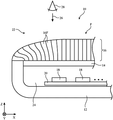
1. An electronic device comprising:
an array of pixels configured to display an image; and
an image transport layer having an input surface and an output surface, wherein the image transport layer is configured to transport the image from the input surface to the output surface and wherein the image transport layer includes a plurality of fibers that each comprise:
a core that extends along a length; and
a light absorbing cladding formed around the core, wherein the light absorbing cladding comprises a transparent polymer and elongated strips of light absorbing material that extend parallel to the length and wherein the elongated strips are distributed around a perimeter of the transparent polymer.
|