| CPC G01N 24/10 (2013.01) [G01R 33/032 (2013.01); G01R 33/32 (2013.01)] | 32 Claims |
|
1. A magnetometry apparatus comprising:
an array of magnetometer pixels, each magnetometer pixel of the array of magnetometer pixels comprising:
a respective electron spin defect body comprising a plurality of lattice point defects, and
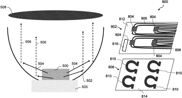
a respective microwave field transmitter configured to apply a microwave field to the electron spin defect body of the magnetometer pixel;
an optical source configured to emit input light of a first wavelength that excites the plurality of lattice point defects of the electron spin defect bodies of the magnetometer pixels of the array of magnetometer pixels from a ground state to an excited state; and
a photodetector arranged to receive photoluminescence of a second wavelength emitted from a plurality of the electron spin defect bodies of the magnetometer pixels of the array of magnetometer pixels,
wherein the photodetector comprises a light collecting pixel array, and wherein the photodetector and the plurality of electron spin defect bodies are arranged such that respective photoluminescences emitted from the plurality of electron spin defect bodies are received at respective distinct portions of the light collecting pixel array, and
wherein the second wavelength is different from the first wavelength.
|