| CPC C23C 14/088 (2013.01) [C04B 35/4682 (2013.01); C04B 35/4686 (2013.01); C23C 14/024 (2013.01); C23C 14/0635 (2013.01); C23C 14/5806 (2013.01); C23C 16/0272 (2013.01); C23C 16/32 (2013.01); C23C 16/409 (2013.01); C23C 16/45531 (2013.01); C23C 16/56 (2013.01); H01L 21/02197 (2013.01); H01L 28/55 (2013.01)] | 8 Claims |
|
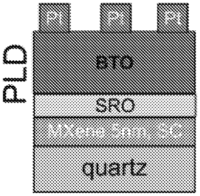
1. A structure comprising: a stacked assembly of a dielectric substrate, a MXene layer, and at least one layer of an oriented-perovskite-structured material,
wherein the perovskite-structured material is disposed on the MXene layer,
wherein the perovskite-structured material has the formula of (i) BaTiO3, (ii) Am−1Bi2MmO3m+3, (iii) Am+1MmO3m+1, or (iv) AmMmO3m+2,
wherein when the perovskite-structured material has the formula of Am−1Bi2MmO3m+3, A=Bi3+, Ba2+, Sr2+, Ca2+, Pb2+, K+, or Na+, and M=Ti4+, Nb5+, Ta5−, Mo6+, W6+, or Fe3+,
wherein when the perovskite-structured material has the formula of Am+1MmO3m+1, A=Bi3+, Ba2+, Sr2+, Ca2+, Pb2+, K+, or Na+and M=Ti4+, Nb5+, Ta5−, Mo6+, W6 +, or Fe3+, and
wherein when the perovskite-structured material has the formula of AmMmO3m+2, A=Bi3+, Ba2+, Sr2+, Ca2+, Pb2+, K+, or Na+, and M=Ti4+, Nb5+, Ta5−, Mo6+, W6+, or Fe3+, and
wherein the MXene layer is sandwiched between the dielectric substrate and the at least one layer of oriented perovskite-structured material.
|