| CPC B64C 29/0033 (2013.01) [B60L 15/02 (2013.01); B64D 27/10 (2013.01); B64D 27/24 (2013.01); B64D 35/04 (2013.01); H02M 7/003 (2013.01); H02M 7/537 (2013.01); H05K 7/1427 (2013.01); H05K 7/209 (2013.01); B60L 2200/10 (2013.01); B60L 2210/30 (2013.01); B64D 2027/026 (2013.01)] | 18 Claims |
|
1. An electrical vertical takeoff and landing (eVTOL) aircraft comprising:
a plurality of electrical propulsion units (EPUs), each EPU of the plurality of EPUs having a propeller or a fan configured to be driven to rotate by an electric motor arranged to receive electrical power from at least one inverter of a plurality of inverters,
wherein each inverter of the plurality of inverters comprises:
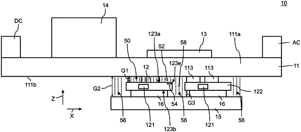
a multi-layer planar carrier substrate defining an x-y direction parallel to a planar surface of the multi-layer planar carrier substrate and a z-direction perpendicular to the x-y direction, the multi-layer planar carrier substrate comprising a plurality of electrically conductive layers extending in the x-y direction and at least one electrical connection extending in the z-direction;
a converter commutation cell comprising a power circuit and a gate driver circuit, the power circuit comprising at least one power semiconductor switching element and at least one capacitor, wherein each power semiconductor switching element of the at least one power semiconductor switching element is comprised in a power semiconductor prepackage, the respective power semiconductor prepackage comprising one or more power semiconductor switching elements embedded in a solid insulating material; and
a heat sink arranged to remove heat from the respective power semiconductor prepackage,
wherein the heat sink is spaced apart in the z-direction from the multi-layer planar carrier substrate so as to define a heat sink gap between the multi-layer planar carrier substrate and the heat sink, and
wherein a converter parameter φ is less than or equal to 20 nm2/V, the converter parameter φ being defined as a size in the z-direction of the heat sink gap divided by a maximum electric field strength in the heat sink gap.
|