| CPC H10B 20/38 (2023.02) | 12 Claims |
|
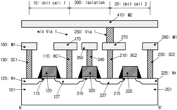
1. A mask-programmable read only memory (ROM), comprising:
a first unit cell and a second unit cell;
an isolation gate electrode configured to isolate the first unit cell and the second unit cell; and
a bit line configured to cross the first unit cell and the second unit cell,
wherein the first unit cell comprises:
a first source region and a first drain region disposed in a semiconductor substrate;
a first gate electrode disposed between the first source region and the first drain region;
a first source contact disposed on the first source region;
a first bit line contact disposed on the first drain region; and
a first metal wiring in contact with the first bit line contact, wherein the first metal wiring extends to overlap a portion of the first gate electrode and does not fully cross the first gate electrode, such that the first metal wiring does not overlap the first source region,
wherein there is no via structure connecting the first metal wiring to the bit line, such that there is no electrical connection between the first drain region and the bit line,
wherein the second unit cell comprises:
a second source region and a second drain region disposed in the semiconductor substrate;
a second gate electrode disposed between the second source region and the second drain region;
a second source contact disposed on the second source region;
a second bit line contact disposed on the second drain region;
a second metal wiring in contact with the second bit line contact, wherein the second metal wiring extends to overlap a portion of the second gate electrode and does not fully cross the second gate electrode, such that the second metal wiring does not overlap the second source region; and
a via structure connecting the second metal wiring to the bit line, wherein the via structure is electrically connected to the second drain region, the second bit line contact, the second metal wiring, and the bit line, and
wherein the bit line is disposed to overlap each of the first bit line contact, the second bit line contact, the first source contact, and the second source contact.
|