US 11,770,963 B2
Display device
Sanghyun Jun, Suwon-si (KR); Kiho Bang, Hwaseong-si (KR); Eunae Jung, Hwaseong-si (KR); Keunlim Ku, Hwaseong-si (KR); and Mi-ran Ji, Hwaseong-si (KR)
Assigned to Samsung Display Co., Ltd., Yongin-si (KR)
Filed by SAMSUNG DISPLAY CO., LTD., Yongin-si (KR)
Filed on May 26, 2022, as Appl. No. 17/826,009.
Application 17/826,009 is a continuation of application No. 17/156,427, filed on Jan. 22, 2021, granted, now 11,348,980.
Application 17/156,427 is a continuation of application No. 16/372,276, filed on Apr. 1, 2019, granted, now 10,930,714, issued on Feb. 23, 2021.
Application 16/372,276 is a continuation of application No. 15/662,105, filed on Jul. 27, 2017, granted, now 10,312,299, issued on Jun. 4, 2019.
Claims priority of application No. 10-2016-0097498 (KR), filed on Jul. 29, 2016.
Prior Publication US 2022/0293690 A1, Sep. 15, 2022
This patent is subject to a terminal disclaimer.
Int. Cl. G06F 3/041 (2006.01); H10K 59/40 (2023.01); G06F 3/044 (2006.01); H10K 50/844 (2023.01); H10K 59/12 (2023.01); H10K 102/00 (2023.01)
CPC H10K 59/40 (2023.02) [G06F 3/044 (2013.01); G06F 3/0412 (2013.01); G06F 3/0443 (2019.05); G06F 3/0446 (2019.05); H10K 50/844 (2023.02); H10K 50/8445 (2023.02); G06F 3/04164 (2019.05); G06F 2203/04102 (2013.01); G06F 2203/04107 (2013.01); G06F 2203/04111 (2013.01); G06F 2203/04112 (2013.01); H10K 59/12 (2023.02); H10K 2102/311 (2023.02)] 20 Claims
OG exemplary drawing
 
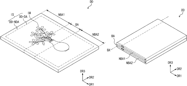
1. A display device comprising:
a display panel comprising a base layer, a circuit layer on the base layer, a light emitting layer on the circuit layer, and a thin film sealing layer on the light emitting layer and comprising a first inorganic layer, an organic layer on the first inorganic layer, and a second inorganic layer on the organic layer; and
a sensor directly on the display panel and comprising a first touch pattern and a second touch pattern spaced from the first touch pattern,
wherein a first gap between a first portion of the first touch pattern and the base layer is smaller than a second gap between the second touch pattern and the base layer.