| CPC H10B 43/40 (2023.02) [H01L 23/5226 (2013.01); H10B 41/27 (2023.02); H10B 41/41 (2023.02); H10B 43/27 (2023.02)] | 20 Claims |
|
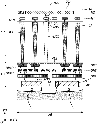
1. A memory device comprising:
a substrate defined with a first cell region and a second cell region, disposed in a first direction, and a row decoder region disposed between the first cell region and the second cell region;
a peripheral circuit defined in the first and second cell regions of the substrate;
a plurality of pass transistors defined in the row decoder region of the substrate;
a plurality of bottom wiring layers disposed in a first dielectric layer, which covers the peripheral circuit and the plurality of pass transistors;
a memory cell array defined on the first dielectric layer;
a second dielectric layer, defined on the first dielectric layer, that covers the memory cell array;
a plurality of top wiring layers disposed in a third dielectric layer, which is defined on the second dielectric layer; and
a plurality of global lines, disposed in the row decoder region, that transfer operating voltages to the plurality of pass transistors,
wherein the plurality of global lines are disposed only in a bottom wiring layer from among the plurality of bottom wiring layers and the plurality of top wiring layers.
|