| CPC H05K 3/32 (2013.01) [H05K 1/0296 (2013.01); H05K 1/05 (2013.01); H05K 2201/03 (2013.01); H05K 2201/095 (2013.01)] | 20 Claims |
|
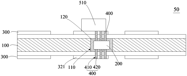
1. A circuit board, comprising:
a substrate, defining a first through-hole;
a metal block, embedded in the first through-hole and fixedly connected to the substrate;
a conductive line layer, arranged on at least one side surface of the substrate; wherein the conductive line layer partially covers an opening of the first through-hole on a corresponding side surface of the substrate; and
a conductive channel, penetrating the conductive line layer and extending to the metal block;
wherein the conductive line layer defines at least one third through-hole corresponding to the conductive channel; the conductive channel comprises a second through-hole and a conductive medium plated on a wall of the second through-hole; and an end of the conductive medium is connected to the conductive line layer, and another end of the conductive medium is connected to the metal block.
|