| CPC H04N 23/80 (2023.01) [G06T 1/60 (2013.01); G06T 5/005 (2013.01); G06V 10/40 (2022.01)] | 20 Claims |
|
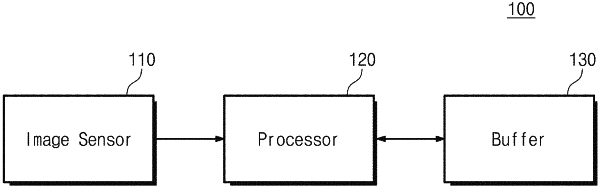
1. An image processing device comprising:
a buffer; and
processing circuitry configured to cause the image processing device to,
first detect a first bad pixel pattern based on first image data,
correct the first bad pixel pattern based on a plurality of first values of a plurality of first peripheral pixels in response to the first detection to obtain a first correction result, the plurality of first peripheral pixels being peripheral to the first bad pixel pattern,
second detect the first bad pixel pattern and a second bad pixel pattern based on the first image data, the second bad pixel pattern being adjacent to the first bad pixel pattern,
correct the second bad pixel pattern based on a plurality of second values of a plurality of second peripheral pixels to obtain a second correction result, the plurality of second peripheral pixels being peripheral to the second bad pixel pattern,
correct the first bad pixel pattern by using the first correction result stored in the buffer in response to the second detection,
generate first correction image data associated with a pattern, the pattern comprising the first bad pixel pattern or the second bad pixel pattern, and
store the first correction image data in the buffer.
|