| CPC H03K 17/0812 (2013.01) [H03K 17/0412 (2013.01); H03K 2217/0036 (2013.01)] | 15 Claims |
|
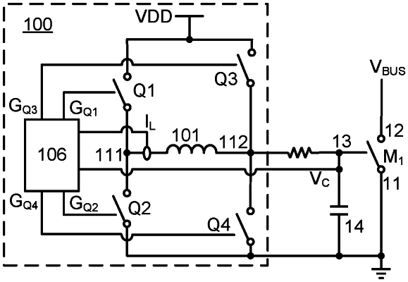
1. A power switch device driver, configured to drive a controllable power switch device to operate between ON and OFF, the controllable power switch device having a first terminal, a second terminal, a control terminal, and an effective capacitor formed between the first terminal and the control terminal, the power switch device driver comprising:
a first switch, coupled between a power supply and a first end of an inductor;
a second switch, coupled between a voltage reference and the first end of the inductor;
a third switch, coupled between the power supply and a second end of the inductor;
a fourth switch, coupled between the voltage reference and the second end of the inductor; and
a logical controller, configured to control the first switch, the second switch, the third switch, and the fourth switch in response to a logical control signal, an inductor current, and a voltage across the effective capacitor; wherein when the logical control signal goes high, the logical controller is configured to control the first switch to be ON, and control the second switch, the third switch, and the fourth switch to be OFF to charge the effective capacitor; and wherein
the logical controller is further configured to control the second switch to be ON, and control the first switch, the third switch, and the fourth switch to be OFF when the logical control signal goes low, to discharge the effective capacitor.
|