| CPC H02M 3/33569 (2013.01) [H02M 1/342 (2021.05); H02M 1/38 (2013.01); H02M 3/33523 (2013.01)] | 10 Claims |
|
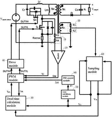
1. A system for controlling an active clamp flyback (ACF) converter, the ACF converter comprising a transformer primary side and a transformer secondary side, the primary side comprising a primary winding, a main switching transistor and a clamp switching transistor, and the system comprising:
a drive module configured to control turning-on or turning-off of the main switching transistor and the clamp switching transistor;
a main switching transistor voltage sampling circuit configured to sample a voltage drop between an input terminal and an output terminal of the main switching transistor;
a first comparator connected to the main switching transistor voltage sampling circuit and configured to determine whether a sampled first sampling voltage is a positive voltage or a negative voltage;
a dead-time calculation module configured to adjust, according to an output of the first comparator and a main switching transistor control signal of a current cycle, a clamp switching transistor control signal of next cycle outputted by the drive module; the adjusting comprising decreasing a high-level duration of the clamp switching transistor control signal of the next cycle when a rising edge of the main switching transistor control signal of the current cycle comes ahead of the negative voltage, and increasing the high-level duration of the clamp switching transistor control signal of the next cycle when the rising edge comes at an end of the negative voltage; and
an excitation inductor;
wherein the dead-time calculation module is further configured to calculate a first dead time according to the voltage drop, an inductance value of the excitation inductor, a parasitic capacitance value of the main switching transistor, a peak current of the excitation inductor and an input voltage value of the flyback converter, and the first dead time is a time from the turning-off of the main switching transistor to the turning-on of the clamp switching transistor; and
wherein the drive module is further configured to control the turning-on or the turning-off of the main switching transistor and the clamp switching transistor according to the first dead time;
the system further comprising an auxiliary winding, an auxiliary winding sampling circuit and a sampling module, the auxiliary winding sampling circuit being configured to sample a voltage of the auxiliary winding and output a sampled second sampling voltage to the sampling module, and the sampling module being configured to calculate and output an output voltage value of the flyback converter and an input voltage value of the flyback converter to the dead-time calculation module;
the sampling module comprising a second comparator, a third comparator and a sampling calculation module;
a positive input terminal of the second comparator is configured to input the second sampling voltage, and a negative input terminal thereof is configured to input the output voltage value of the flyback converter outputted by the sampling calculation module;
a positive input terminal of the third comparator is configured to input the second sampling voltage, and a negative input terminal thereof is configured to input the input voltage value of the flyback converter outputted by the sampling calculation module;
the sampling calculation module is configured to calculate and output the input voltage value of the flyback converter and the output voltage value of the flyback converter, compare a high-level duration of an output of the second comparator in the current cycle with a first preset reference duration, increase the output voltage value of the flyback converter of the next cycle outputted by the sampling calculation module if the high-level duration is greater than the first preset reference duration, and decrease the output voltage value of the flyback converter of the next cycle outputted by the sampling calculation module if the high-level duration is less than the first preset reference duration; and
the sampling calculation module is further configured to compare a high-level duration of an output of the third comparator in the current cycle with a second preset reference duration, increase the input voltage value of the flyback converter of the next cycle outputted by the sampling calculation module if the high-level duration of the output of the third comparator in the current cycle is greater than the second preset reference duration, and decrease the input voltage value of the flyback converter of the next cycle outputted by the sampling calculation module if the high-level duration of the output of the third comparator in the current cycle is less than the second preset reference duration.
|