| CPC H01L 33/06 (2013.01) [H01L 25/167 (2013.01); H01L 27/156 (2013.01); H01L 33/005 (2013.01); H01L 33/0075 (2013.01); H01L 33/10 (2013.01); H01L 33/20 (2013.01); H01L 33/382 (2013.01); H01L 33/42 (2013.01); H01L 33/465 (2013.01); H01L 33/502 (2013.01); H01L 33/60 (2013.01); B82Y 20/00 (2013.01); B82Y 40/00 (2013.01); H01L 2933/0025 (2013.01); H01L 2933/0041 (2013.01)] | 18 Claims |
|
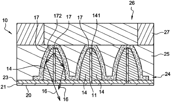
1. A manufacturing method for manufacturing an optoelectronic device including an array of light-emitting diodes, including the following steps:
formation of the array of light-emitting diodes on a support face of a substrate, this step being carried out so that each light-emitting diode of the array of light-emitting diodes has an elongate wire-like shape according to a longitudinal axis extending according to a transverse direction of the optoelectronic device directed transversely to the support face of the substrate,
formation of spacing walls made of a first dielectric material transparent to light radiation originating from each light-emitting diode of the array of light-emitting diodes such that lateral sidewalls of each light-emitting diode of the array of light-emitting diodes, over an entire height thereof considered according to the transverse direction, are surrounded by at least one of the spacing walls,
formation of light confinement walls made of a second material adapted to block the light radiation originating from each light-emitting diode of the array of light-emitting diodes that directly cover lateral sidewalls of the spacing walls by being in contact with the lateral sidewalls of the spacing walls, so that the light radiation originating from each light-emitting diode of the array of light-emitting diodes and directed in a direction of an adjacent light-emitting diode of the array of light-emitting diodes is blocked by a light confinement wall of the light confinements walls which covers a spacing wall of the spacing walls that surrounds a respective one of each light-emitting diode of the array of light-emitting diodes,
wherein at the end of the step of formation of the light confinement walls, an upper border of each light-emitting diode of the array of light-emitting diodes is covered by a light confinement wall so that after implementation of a step of removing the substrate, the light radiation originating from the light-emitting diodes of the array of light-emitting diodes is emitted out of the optoelectronic device by an emission surface of the optoelectronic device located, with respect to the light-emitting diodes of the array of light-emitting diodes, on a side opposite to upper border of the light-emitting diodes of the array of light-emitting diodes according to the transverse direction, wherein the step of formation of the spacing walls is implemented so that the spacing walls have an outer face with a convex shape, and wherein each light confinement wall has an inner face having a concave shape matching with the convex shape and directed towards a light-emitting diode of the array of light-emitting diodes for which each light confinement wall confines the light radiation thereof.
|