US 11,769,837 B2
Semiconductor device
Yu-Chu Lin, Tainan (TW); Chi-Chung Jen, Kaohsiung (TW); Wen-Chih Chiang, Hsinchu (TW); Ming-Hong Su, Tainan (TW); Yung-Han Chen, Taichung (TW); Mei-Chen Su, Kaohsiung (TW); and Chia-Ming Pan, Tainan (TW)
Assigned to Taiwan Semiconductor Manufacturing Company, Ltd., Hsinchu (TW)
Filed by Taiwan Semiconductor Manufacturing Company, Ltd., Hsinchu (TW)
Filed on Jan. 28, 2022, as Appl. No. 17/586,898.
Application 17/586,898 is a continuation of application No. 17/100,562, filed on Nov. 20, 2020, granted, now 11,257,963.
Prior Publication US 2022/0165877 A1, May 26, 2022
This patent is subject to a terminal disclaimer.
Int. Cl. H01L 29/78 (2006.01); G11C 16/14 (2006.01); H01L 29/788 (2006.01); H01L 29/66 (2006.01); H10B 41/10 (2023.01); H10B 41/35 (2023.01)
CPC H01L 29/788 (2013.01) [G11C 16/14 (2013.01); H01L 29/66825 (2013.01); H10B 41/10 (2023.02); H10B 41/35 (2023.02)] 20 Claims
OG exemplary drawing
 
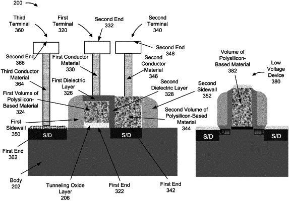
1. A semiconductor device comprising:
a body;
a first terminal, coupled to the body, comprising:
a tunneling oxide layer,
a first gate, and
a first dielectric layer;
a second terminal, coupled to the body, comprising:
a second gate formed directly on the body; and
a second dielectric layer formed between the first gate and the second gate.