| CPC H01L 29/4236 (2013.01) [H01L 29/401 (2013.01); H01L 29/42364 (2013.01)] | 20 Claims |
|
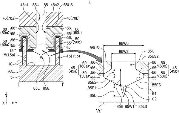
1. A semiconductor device, comprising:
a first active fin and a second active fin disposed on a substrate;
an insulating layer disposed between the first active fin and the second active fin and on the substrate;
first active layers on the first active fin, the first active layers being spaced apart from each other in a vertical direction perpendicular to an upper surface of the substrate;
second active layers on the second active fin, the second active layers being spaced apart from each other in the vertical direction;
a first gate structure intersecting the first active layers and extending in a first direction, the first gate structure surrounding each of the first active layers;
a second gate structure intersecting the second active layers and extending in the first direction, the second gate structure surrounding each of the second active layers; and
a separation structure disposed between the first gate structure and the second gate structure, and extending into the insulating layer,
wherein the first gate structure has a first end portion disposed on the insulating layer;
wherein the second gate structure has a second end portion facing the first end portion of the first gate structure in the first direction,
wherein the first gate structure includes a first gate dielectric structure and a first gate electrode structure on the first gate dielectric structure,
wherein the second gate structure includes a second gate dielectric structure and a second gate electrode structure on the second gate dielectric structure,
wherein the separation structure contacts the first end portion of the first gate structure, the second end portion of the second gate structure, and the insulating layer,
wherein the separation structure includes a maximum width portion, a lower portion below the maximum width portion and contacting the insulating layer, and an upper portion on the maximum width portion, and
wherein the maximum width portion includes a first portion between the first gate electrode structure and the insulating layer, a second portion between the second gate electrode structure and the insulating layer, and a third portion between the first portion and the second portion.
|