| CPC H01L 27/0886 (2013.01) [H01L 21/26513 (2013.01); H01L 21/761 (2013.01); H01L 21/76224 (2013.01); H01L 21/76877 (2013.01); H01L 21/823431 (2013.01); H01L 21/823475 (2013.01); H01L 21/823481 (2013.01); H01L 23/528 (2013.01); H01L 27/0207 (2013.01); H01L 29/0646 (2013.01); H01L 29/0649 (2013.01); H01L 29/0653 (2013.01); H01L 29/0847 (2013.01); H01L 29/41775 (2013.01); H01L 29/41791 (2013.01); H01L 29/6656 (2013.01); H01L 29/66545 (2013.01); H01L 29/785 (2013.01); H01L 29/7854 (2013.01)] | 19 Claims |
|
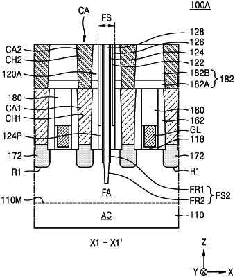
1. An integrated circuit device comprising:
a fin-type active region extending on a substrate in a first horizontal direction;
a gate line extending on the fin-type active region in a second horizontal direction intersecting the first horizontal direction;
a source/drain region in the fin-type active region at one side of the gate line; and
a fin isolation insulating unit vertically extending into the fin-type active region,
wherein the fin isolation insulating unit comprises an upper portion over the fin-type active region and a lower portion buried in the fin-type active region, the upper portion facing the gate line in the first horizontal direction, the lower portion having a round-shaped sidewall, and
wherein the lower portion of the fin isolation insulating unit comprises a maximum width defined by the round-shaped sidewall in the first horizontal direction at a level lower than a bottom of the source/drain region.
|