| CPC H01L 25/0657 (2013.01) [H01L 23/367 (2013.01); H01L 23/3736 (2013.01); H01L 24/49 (2013.01); H10B 12/00 (2023.02)] | 11 Claims |
|
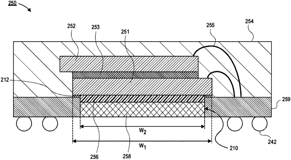
1. An electronics package, comprising:
a package substrate;
a first die coupled to the package substrate, the first die having a bottommost surface above an uppermost surface of an entirety of the package substrate;
a second die over the first die, wherein the first die and the second die are electrically coupled to the package substrate with wire bonds;
a cavity through the package substrate, wherein the cavity is within a footprint of the first die; and
a thermal stack in the cavity, wherein the thermal stack directly physically contacts the first die, and wherein the thermal stack is within the footprint of the first die.
|