| CPC H01L 24/14 (2013.01) [H01L 21/563 (2013.01); H01L 23/481 (2013.01); H01L 24/05 (2013.01); H01L 24/10 (2013.01); H01L 24/11 (2013.01); H01L 24/12 (2013.01); H01L 24/13 (2013.01); H01L 24/73 (2013.01); H01L 24/03 (2013.01); H01L 24/06 (2013.01); H01L 2224/0345 (2013.01); H01L 2224/03912 (2013.01); H01L 2224/0401 (2013.01); H01L 2224/05022 (2013.01); H01L 2224/05025 (2013.01); H01L 2224/0557 (2013.01); H01L 2224/05155 (2013.01); H01L 2224/05166 (2013.01); H01L 2224/05171 (2013.01); H01L 2224/05572 (2013.01); H01L 2224/05582 (2013.01); H01L 2224/05644 (2013.01); H01L 2224/05647 (2013.01); H01L 2224/05655 (2013.01); H01L 2224/0603 (2013.01); H01L 2224/06102 (2013.01); H01L 2224/10125 (2013.01); H01L 2224/1147 (2013.01); H01L 2224/11462 (2013.01); H01L 2224/11849 (2013.01); H01L 2224/12105 (2013.01); H01L 2224/131 (2013.01); H01L 2224/13025 (2013.01); H01L 2224/13082 (2013.01); H01L 2224/13111 (2013.01); H01L 2224/13144 (2013.01); H01L 2224/13147 (2013.01); H01L 2224/13155 (2013.01); H01L 2224/13564 (2013.01); H01L 2224/13582 (2013.01); H01L 2224/14104 (2013.01); H01L 2224/14515 (2013.01); H01L 2224/14517 (2013.01); H01L 2224/26145 (2013.01); H01L 2224/73104 (2013.01); H01L 2224/81191 (2013.01); H01L 2224/81203 (2013.01); H01L 2224/81815 (2013.01)] | 20 Claims |
|
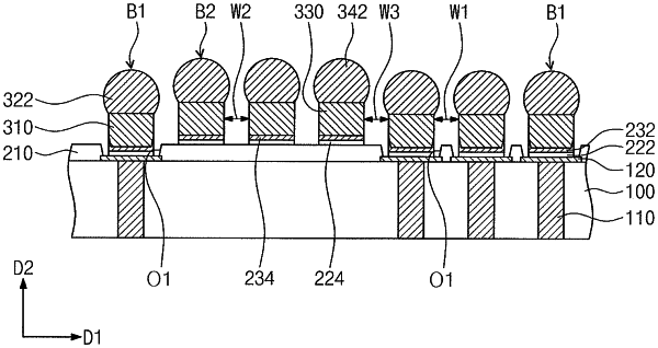
1. A semiconductor package, comprising:
a substrate;
through-electrodes penetrating the substrate;
first bumps spaced apart from each other in a first direction parallel to a top surface of the substrate, the first bumps being electrically connected to the through-electrodes, respectively;
at least one second bump disposed between the first bumps, the at least one second bump being electrically floated; and
an underfill covering the substrate, the first bumps, and the at least one second bump,
wherein the first bumps and the at least one second bump constitute one row in the first direction, and
wherein the at least one second bump is disposed at a higher level from the substrate than the first bumps.
|