| CPC H01L 24/08 (2013.01) [H01L 24/05 (2013.01); H01L 24/13 (2013.01); H01L 2224/0401 (2013.01); H01L 2224/05009 (2013.01); H01L 2224/05557 (2013.01); H01L 2224/08059 (2013.01); H01L 2224/13021 (2013.01); H01L 2924/35121 (2013.01)] | 20 Claims |
|
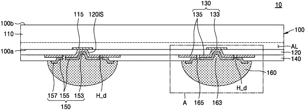
1. A semiconductor package comprising:
a semiconductor chip comprising a chip pad on a first surface of the semiconductor chip;
a first insulating layer arranged on the semiconductor chip and comprising an insulating hole exposing the chip pad;
a redistribution pattern comprising a redistribution via pattern arranged on an internal surface of the first insulating layer that is configured to define the insulating hole and on a surface of the chip pad, and a redistribution line pattern arranged on a surface of the first insulating layer to extend in a horizontal direction and comprising a first dummy hole;
an under bump metal (UBM) comprising a first UBM portion arranged on the redistribution via pattern and a second UBM portion extending from the first UBM portion to be arranged on the redistribution line pattern and comprising a second dummy hole overlapping the first dummy hole in a vertical direction; and
a connection terminal arranged on the UBM, and comprising a dummy portion configured to fill an internal portion of a dummy hole comprising the first dummy hole of the redistribution line pattern and the second dummy hole of the second UBM portion.
|