| CPC H01L 24/05 (2013.01) [H01L 2224/05583 (2013.01)] | 20 Claims |
|
1. A method of manufacturing a semiconductor chip, the method comprising:
preparing a semiconductor substrate;
forming a top connection pad in a top surface; and
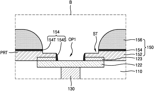
forming a protection insulation layer having an opening therein, the protection insulation layer not covering at least a portion of the top connection pad, on the semiconductor substrate,
wherein the protection insulation layer includes:
a bottom protection insulation layer,
a cover insulation layer comprising a side cover part that covers at least a portion of a side surface of the bottom protection insulation layer and a top cover part disposed apart from the side cover part to cover at least a portion of a top surface of the bottom protection insulation layer, and
a top protection insulation layer formed of a photosensitive polyimide, and disposed on the top cover part.
|